LTC4232
9
4232fa
applicaTions inForMaTion
This gate slope is designed to charge up a 1000礔 capaci-
tor to 12V in 40ms, with an inrush current of 300mA. This
allows the inrush current to stay under the current limit
threshold (1.5A) for capacitors less than 1000礔. Included
in the Typical Performance Characteristics section is a
graph of the Safe Operating Area for the MOSFET. It is
evident from this graph that the power dissipation at 12V,
300mA for 40ms is in the safe region.
Adding a capacitor and a 1k series resistor from GATE to
ground will lower the inrush current below the default value
set by the INRUSH circuit. The GATE is charged with an
24礎 current source (when INRUSH circuit is not driving
the GATE). The voltage at the GATE pin rises with a slope
equal to 24礎/C
GATE
and the supply inrush current is set at:
I
INRUSH
=
C
L
C
GATE
" 24礎
When the GATE voltage reaches the MOSFET threshold
voltage, the switch begins to turn on and the OUT volt-
age follows the GATE voltage as it increases. Once OUT
reaches V
DD
, the GATE will ramp up until clamped by the
6.15V Zener between GATE and OUT.
As the OUT voltage rises, so will the FB pin which is moni-
toring it. Once the FB pin crosses its 1.235V threshold
and the GATE to OUT voltage exceeds 4.2V, the PG pin
will cease to pull low and indicate that the power is good.
Parasitic MOSFET Oscillation
When the N-channel MOSFET ramps up the output during
power-up it operates as a source follower. The source
follower configuration may self-oscillate in the range of
25kHz to 300kHz when the load capacitance is less than
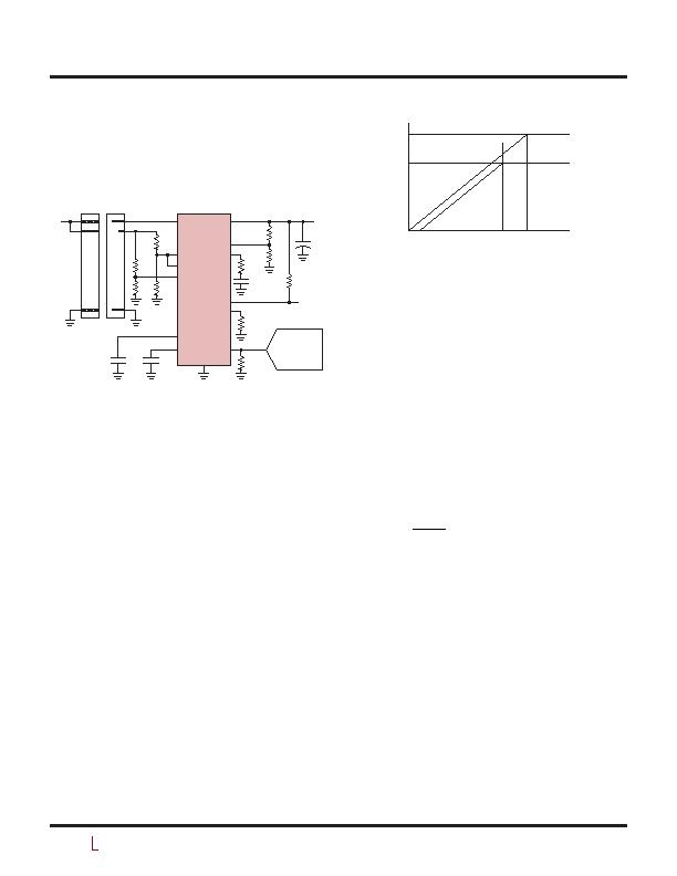
Figure 2. Supply Turn-On
Figure 1. 2A, 12V Card Resident Application
The typical LTC4232 application is in a high availability
system that uses a positive voltage supply to distribute
power to individual cards. A complete application circuit
is shown in Figure 1. External component selection is
discussed in detail in the following sections.
ADC
R1
226k
C1
0.1礔
R2
20k
12V
4232 F01
C
T
0.1礔
C
L
330礔
V
OUT
12V
2A
V
DD
UV
OUT
FB
PG
GND
I
MON
R
SET
20k
R
MON
20k
I
SET
C
GATE
0.1礔
R
GATE
1k
GATE
LTC4232
OV
INTV
CC
TIMER
FLT
+
R3
140k
R4
20k
R7
10k
R6
20k
R5
150k
t1
t2
SLOPE = 0.3V/ms
GATE
OUT
V
DD
+ 6.15
V
DD
4232 F02
Turn-On Sequence
Several conditions must be present before the internal
pass MOSFET can be turned on. First the supply V
DD
must
exceed its undervoltage lockout level. Next the internally
generated supply INTV
CC
must cross its 2.65V undervolt-
age threshold. This generates a 25祍 power-on-reset pulse
which clears the fault register and initializes internal latches.
After the power-on-reset pulse, the LTC4232 will go
through the following sequence. First, the UV and OV pins
must indicate that the input voltage is within the accept-
able range. All of these conditions must be satisfied for
the duration of 100ms to ensure that any contact bounce
during the insertion has ended.
The MOSFET is turned on by charging up the GATE with
a charge pump generated current source whose value is
adjusted by shunting a portion of the pull-up current to
ground. The charging current is controlled by the INRUSH
circuit that maintains a constant slope of GATE voltage
versus time (Figure 2). The voltage at the GATE pin rises
with a slope of 0.3V/ms and the supply inrush current is
set at:
I
INRUSH
= C
L
" (0.3V/ms)
发布紧急采购,3分钟左右您将得到回复。
相关PDF资料
LTC4240IGN#TRPBF
IC CTRLR HOTSWAP CPCI I2C 28SSOP
LTC4241IGN#PBF
IC CTRLR HOTSWAP 3.3V AUX 20SSOP
LTC4242CUHF#TRPBF
IC CNTRLR HOT SWAP 38-QFN
LTC4244CGN-1#TRPBF
IC CTRLR HOTSWAP PCI 20-SSOP
LTC4245CG#TRPBF
IC CNTRLR HOT SWAP 36-SSOP
LTC4251-2CS6#TRPBF
IC CTRLR HOTSWAP NEGVOLT SOT23-6
LTC4252A-1IMS#TRPBF
IC CNTRLR HOTSWAP NEGVOLT 10MSOP
LTC4253ACGN#TRPBF
IC HOT SWAP CONTRLR -48V 16-SSOP
相关代理商/技术参数
LTC4232IDHC#PBF
功能描述:IC CTLR HOT SWAP 5A 16-DFN RoHS:是 类别:集成电路 (IC) >> PMIC - 热交换 系列:- 产品培训模块:Lead (SnPb) Finish for COTS
Obsolescence Mitigation Program 标准包装:119 系列:- 类型:热交换控制器 应用:通用型,PCI Express? 内部开关:无 电流限制:- 电源电压:3.3V,12V 工作温度:-40°C ~ 85°C 安装类型:表面贴装 封装/外壳:80-TQFP 供应商设备封装:80-TQFP(12x12) 包装:托盘 产品目录页面:1423 (CN2011-ZH PDF)
LTC4232IDHC#TRPBF
功能描述:IC CTLR HOT SWAP 5A 16-DFN RoHS:是 类别:集成电路 (IC) >> PMIC - 热交换 系列:- 产品培训模块:Lead (SnPb) Finish for COTS
Obsolescence Mitigation Program 标准包装:119 系列:- 类型:热交换控制器 应用:通用型,PCI Express? 内部开关:无 电流限制:- 电源电压:3.3V,12V 工作温度:-40°C ~ 85°C 安装类型:表面贴装 封装/外壳:80-TQFP 供应商设备封装:80-TQFP(12x12) 包装:托盘 产品目录页面:1423 (CN2011-ZH PDF)
LTC4240
制造商:LINER 制造商全称:Linear Technology 功能描述:CompactPCI Hot Swap Controller with I2C Compatible Interface
LTC4240CGN
功能描述:IC CTRLR HOTSWAP CPCI I2C 28SSOP RoHS:否 类别:集成电路 (IC) >> PMIC - 热交换 系列:- 产品培训模块:Lead (SnPb) Finish for COTS
Obsolescence Mitigation Program 标准包装:119 系列:- 类型:热交换控制器 应用:通用型,PCI Express? 内部开关:无 电流限制:- 电源电压:3.3V,12V 工作温度:-40°C ~ 85°C 安装类型:表面贴装 封装/外壳:80-TQFP 供应商设备封装:80-TQFP(12x12) 包装:托盘 产品目录页面:1423 (CN2011-ZH PDF)
LTC4240CGN#PBF
功能描述:IC CTLR HOT SWAP CPCI I2C 28SSOP RoHS:是 类别:集成电路 (IC) >> PMIC - 热交换 系列:- 产品培训模块:Lead (SnPb) Finish for COTS
Obsolescence Mitigation Program 标准包装:119 系列:- 类型:热交换控制器 应用:通用型,PCI Express? 内部开关:无 电流限制:- 电源电压:3.3V,12V 工作温度:-40°C ~ 85°C 安装类型:表面贴装 封装/外壳:80-TQFP 供应商设备封装:80-TQFP(12x12) 包装:托盘 产品目录页面:1423 (CN2011-ZH PDF)
LTC4240CGN#TR
功能描述:IC CTRLR HOT SWAP CPCI 28-SSOP RoHS:否 类别:集成电路 (IC) >> PMIC - 热交换 系列:- 产品培训模块:Lead (SnPb) Finish for COTS
Obsolescence Mitigation Program 标准包装:119 系列:- 类型:热交换控制器 应用:通用型,PCI Express? 内部开关:无 电流限制:- 电源电压:3.3V,12V 工作温度:-40°C ~ 85°C 安装类型:表面贴装 封装/外壳:80-TQFP 供应商设备封装:80-TQFP(12x12) 包装:托盘 产品目录页面:1423 (CN2011-ZH PDF)
LTC4240CGN#TRPBF
功能描述:IC CTRLR HOTSWAP CPCI I2C 28SSOP RoHS:是 类别:集成电路 (IC) >> PMIC - 热交换 系列:- 产品培训模块:Lead (SnPb) Finish for COTS
Obsolescence Mitigation Program 标准包装:119 系列:- 类型:热交换控制器 应用:通用型,PCI Express? 内部开关:无 电流限制:- 电源电压:3.3V,12V 工作温度:-40°C ~ 85°C 安装类型:表面贴装 封装/外壳:80-TQFP 供应商设备封装:80-TQFP(12x12) 包装:托盘 产品目录页面:1423 (CN2011-ZH PDF)
LTC4240IGN
功能描述:IC CTRLR HOT SWAP CPCI 28-SSOP RoHS:否 类别:集成电路 (IC) >> PMIC - 热交换 系列:- 产品培训模块:Lead (SnPb) Finish for COTS
Obsolescence Mitigation Program 标准包装:119 系列:- 类型:热交换控制器 应用:通用型,PCI Express? 内部开关:无 电流限制:- 电源电压:3.3V,12V 工作温度:-40°C ~ 85°C 安装类型:表面贴装 封装/外壳:80-TQFP 供应商设备封装:80-TQFP(12x12) 包装:托盘 产品目录页面:1423 (CN2011-ZH PDF)